This project began as an offshoot of my first contribution
to the 555 design
contest.
Initially, I wanted to make a circuit with blinking LED which would use
no components other than 555s. I was actually successful in
creating astable multivibrators that were built solely from
555
ICs, but unfortunately, their output frequencies were in the range of
kHz. Simply put, they were too fast for blinking LED. And so I asked
myself "hey, what if I made a 555 frequency divider which would lower
the frequency into the Hz range?"
A quick Google search yielded several circuits like this
one...
but I could not use that. It is essentially a mere monostable
multivibrator and it can divide input frequency only thanks to the fact
that it cannot be triggered when it already is in the non-stable state.
In other words, it is not a true frequency divider, it works properly
only in very narrow frequency range. Moreover, it requires a
large
capacitor, which goes against my goal to build it solely from 555
ICs. A somewhat deeper Google search yielded this
circuit - that looked a bit better, but its maximum
operating frequency was very limited.
So
I decided to try a different approach - I asked myself "what is the
simplest true frequency divider?" As I suspected, the answer was the
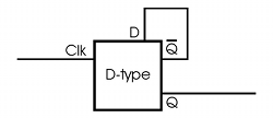
circuit in figure 1.1 - an edge-trigerred D flip-flip which has Q and D signals connected
together (I copied the picture from this
article which also explains how the divider works).
Figure 1.1. D-type frequency
divider
All I had to do was to construct the D
flip-flop from 555s... somehow.
2 555-to-DFF transformation
I've used edge-trigerred D flip-flops in my CPLD and FPGA projects many
times, yet I never realized how complicated their internal structure
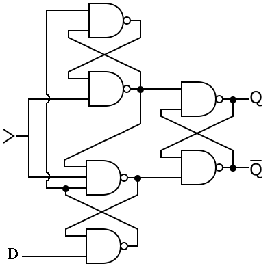
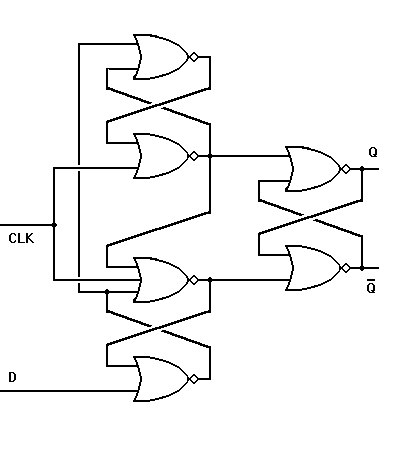
actually was. The flip-flop can be constructed from NAND or NOR gates
and reacts to rising or falling edge of clock signal, respectively. You
will find both versions in figure 2.1. I took the picture with NAND
version from this
Wikipedia page, the picture with NOR version is from this
article (by the way, the article explains in great detail how
the D flip-flop actually works).
a)
b)
Figure 2.1. Edge-triggered D flip-flop made from NAND gates (a)
and from NOR gates (b)
As
is apparent from figure 2.1, the D flip-flop can be built from
three R-S flip-flops... and luckily, one R-S flip-flop can be found
inside every
555 IC! Now, I was uncertain whether the 555 employs NAND-based or
NOR-based R-S flip-flop, but I found the answer pretty quickly - it
reacts to positive pulses from voltage comparators, so it has
to be a NOR-based flip-flop. Unfortunately, the R, S, Q and Q
signals are not directly accessible on 555 pins, which complicates
things a little. Therefore, for the next step, I had to know a detailed
logic model of 555 behavior. I was a bit surprised that someone already
made this - if you want to have really, really in-depth understanding
of the 555 behavior, read this 555
modelling manual written by Mike Brinson.
He presents a model of digital part of 555 on page 6; his
model
even simulates gate propagation delays by RC networks. However, the
model on page 6 describes only digital part of 555; analog parts are
modelled by comparators, transistors etc. like in real
555. This
was a good start, but it was not entirely what I needed
- I
needed to model the entire
555 as a digital circuit. In other words, I needed a model
which would describe 555's behavior if I regarded all
inputs as digital inputs: 0 V representing logic '0' and +5 V
representing logic '1'. Why, you ask? Well, I was trying to build a D
flip-flop, which is a digital circuit!
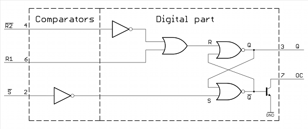
Figure 2.2 Digital model of 555 behavior
Fortunately,
it was really simple to create a digital model of 555 behavior (I used
mr. Brinson's model for starters), you will find it in figure
2.2. The digital part of the 555 is essentially a NOR-based
R-S
flip flop with two reset inputs - one is controlled by THRES comparator
at pin 6 and second
is master reset input at pin 4. The S input is controlled by TRIG
comparator at pin 2.
Now
let's see what happens if we take the comparators into consideration.
The THRES comparator at pin 6 reacts when the input voltage is higher
than 2/3 VCC - which means that +5 V (logic '1')
at this
input translates to logic '1' at the R input of the R-S flip-flop. This
is very good, because from logic standpoint, this comparator is
transparent - hence it can be modelled as simple wire in the
"comparators" box in figure 2.2. But the TRIG comparator at pin 2
reacts only if input voltage is lower than 2/3 VCC
- in
other words, S is logic '1' only when there is logic '0' at
pin
2. So the TRIG comparator behaves like logic invertor and had to be
modelled like that. This unfortunately means that from logic
standpoint, pin 2 is actually S
input of the R-S flip-flop.
The Q output of the R-S flip-flop is connected directly to pin
3. The Q
output of the R-S flip-flop controls the discharge transistor, which is
connected to pin 7; it is essentially an open-collector output.
Unfortunately, pin 7 cannot serve as Q output of the entire
555, because when pin 3 is in logic '1', the transistor is closed.
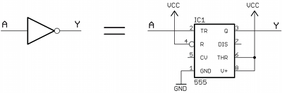
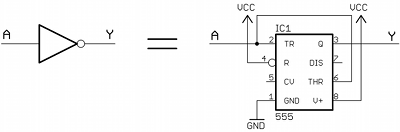
Figure 2.3. 555 as logic inverter
So
from logic standpoint, the 555 behaves like a R-S flip-flop with two
reset inputs, but its set input and one reset input is inverted.
Moreover, it lacks the Q
output. But
to build the D flip-flop from figure 2.1b, I had to correct these
shortcomingst. And there was a really simple way to correct
them -
I had to add inverters to the affected signals/pins. It is fairly easy
to build an inverter from 555, one possible schematic is in figure 2.3.
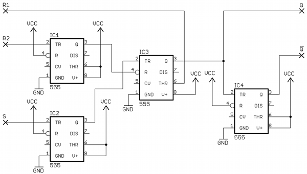
All I had to do now was to put it all together and create a R-S
flip-flop which would have three inputs R1, R2, S and outputs Q and Q.
The result is schematic in figure 2.4 - here IC1, IC2 and IC4 are just
inverters and IC3 serves as the actual flip-flip. I tested this R-S
flip-flop on solderless breadboard and it worked exactly as
it should
- a positive pulse on the S input set the Q output to logic '1',
whereas positive pulse on R1 or R2 input set it to logic
'0'.
Figure 2.4. Complete R-S flip-flop built from 555s
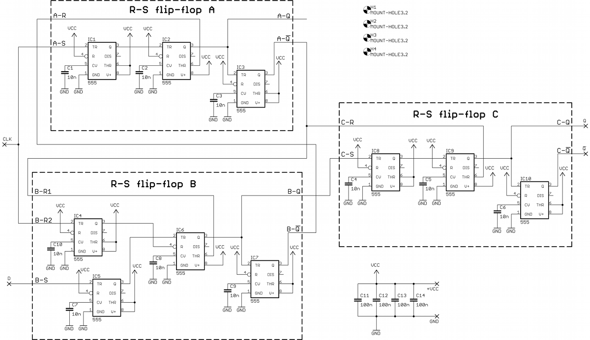
Finally,
it was the time to build an actual edge-trigerred D flip-flop from
three these R-S flip-flops according to schematic in figure 2.1b. The
resulting schematic is in figure 2.5. As you can see, it uses ten 555s,
so I highlighed the individual R-S flip-flops and their inputs
and
outputs, so you could better see what role every 555 plays in it.
Moreover, the schematic has the same layout as in figure 2.1b. Two R-S
flip-flops (named A and C in figure 2.5) need just one reset input, so
they have only two inverters; the second reset input (pin 4) of IC2 and
IC9 is
permanently connected to VCC.
Of course, I tested the circuit from figure 2.5 on solderless
breadboard. It really worked,
but only in static mode. When I connected the Q
output to D input to make the frequency divider, severe
oscillations appeared at both
outputs when the CLK input was held low.Now,
my test circuit
on solderless breadboard
was really a mess; there was a very real possibility that those
oscillations could have been caused by various parasitic couplings on
the breadboard. So I decided to create a test PCB which would allow me
to test the D flip-flop properly. Just to be sure, I added
decoupling capacitors to it - it was easier than doing a new PCB in
case the capacitors were really needed. This is the reason why you can
see all those decoupling capacitors in figure 2.5, even though I
originally planned to make the D flip-flop solely from 555s.
By the way, if you want to try this yourself, build your D flip-flop exactly
as is in figure 2.5, otherwise it might not work. For example, the D
flip-flop will not work properly if you swap the R1 and R2 inputs of
the bottom R-S flip-flop. This is because the 555 reset inputs are not
equal; in some datasheets, you will find a line like this: RESET can override TRIG, which
can override THRES.
Moreover, I strongly recommend
using CMOS 555s
in the flip-flop! It worked most reliably with TLC555CP,
it behaved practically like "real" integrated D flip-flop. With
LMC555CN, it was somewhat unpredictable - for instance, it failed to
work when I simply swapped some ICs! I found out that IC4 is especially
sensitive - it worked with some LMC555CNs, with others it
failed.
The flip-flop was practically useless with TI's bipolar
NE555P,
it behaved more like random state generator than flip-flop with these
ICs. And with National Semiconductor LM555N,
it didn't work at all - for
some reason, not even the inverters worked with these ICs! I think
National implemented the internal logic of these ICs differently,
though I'm not sure exactly what this difference is.
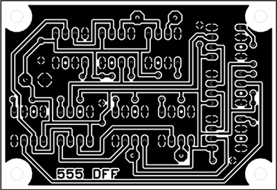
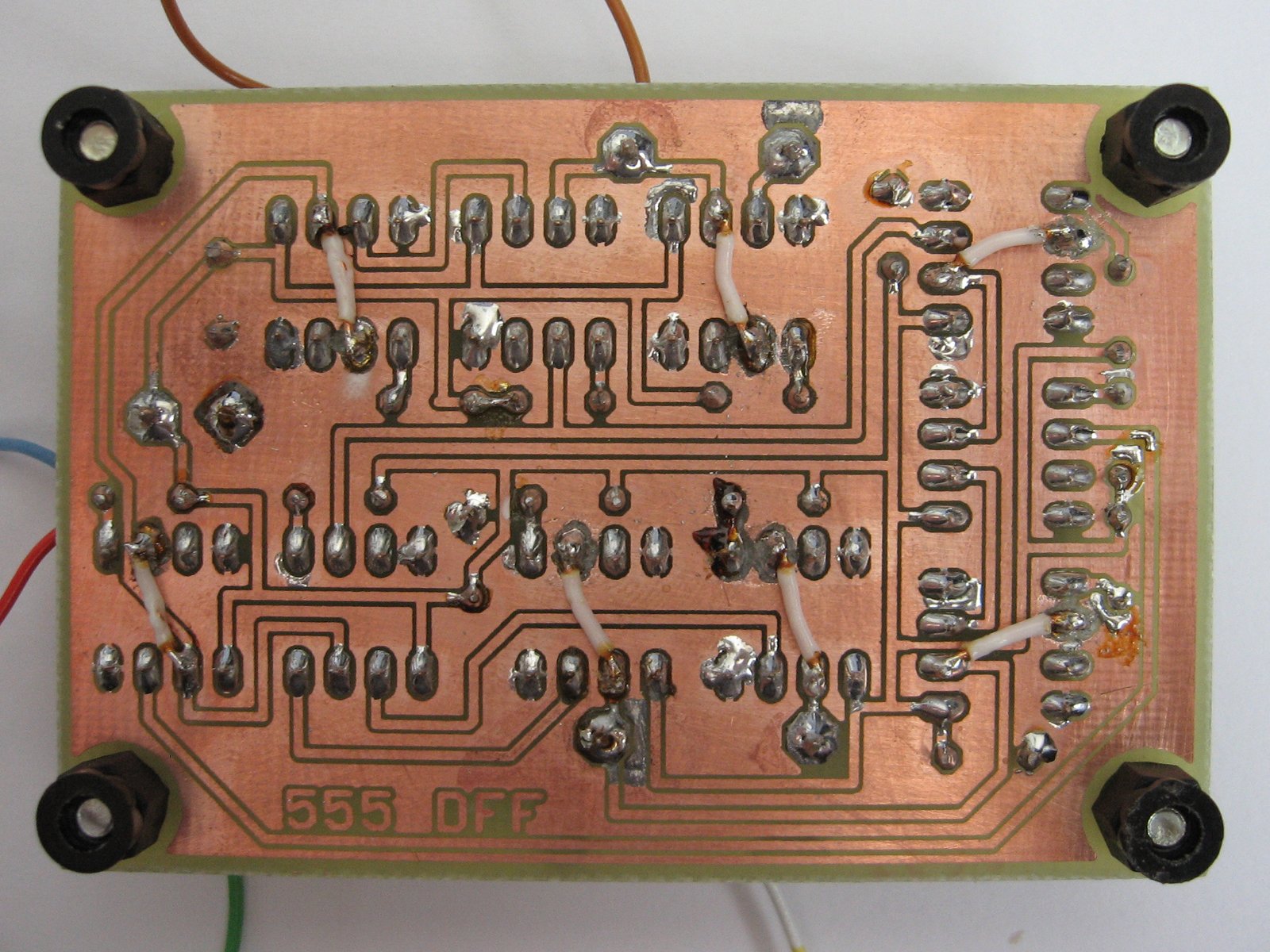
3 D flip-flop test board
So
as I said, I created a test PCB to test the DFF properly, see figures
3.1 and 3.2. I made it in
freeware Eagle 5.11, you can download the source files here .
The board employs a polygon to distribute VCC (instead of GND) - I
chose this simply because many more 555 pins are connected to VCC.
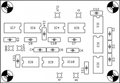
Figure 3.1. Layout of D flip-flop test
board
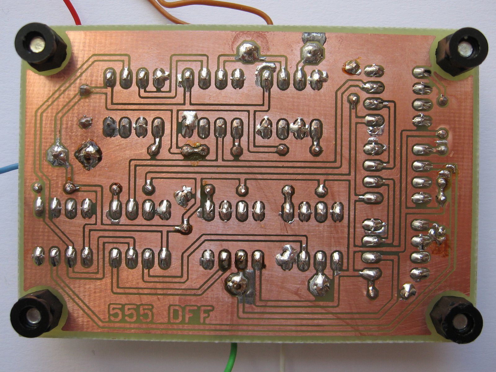
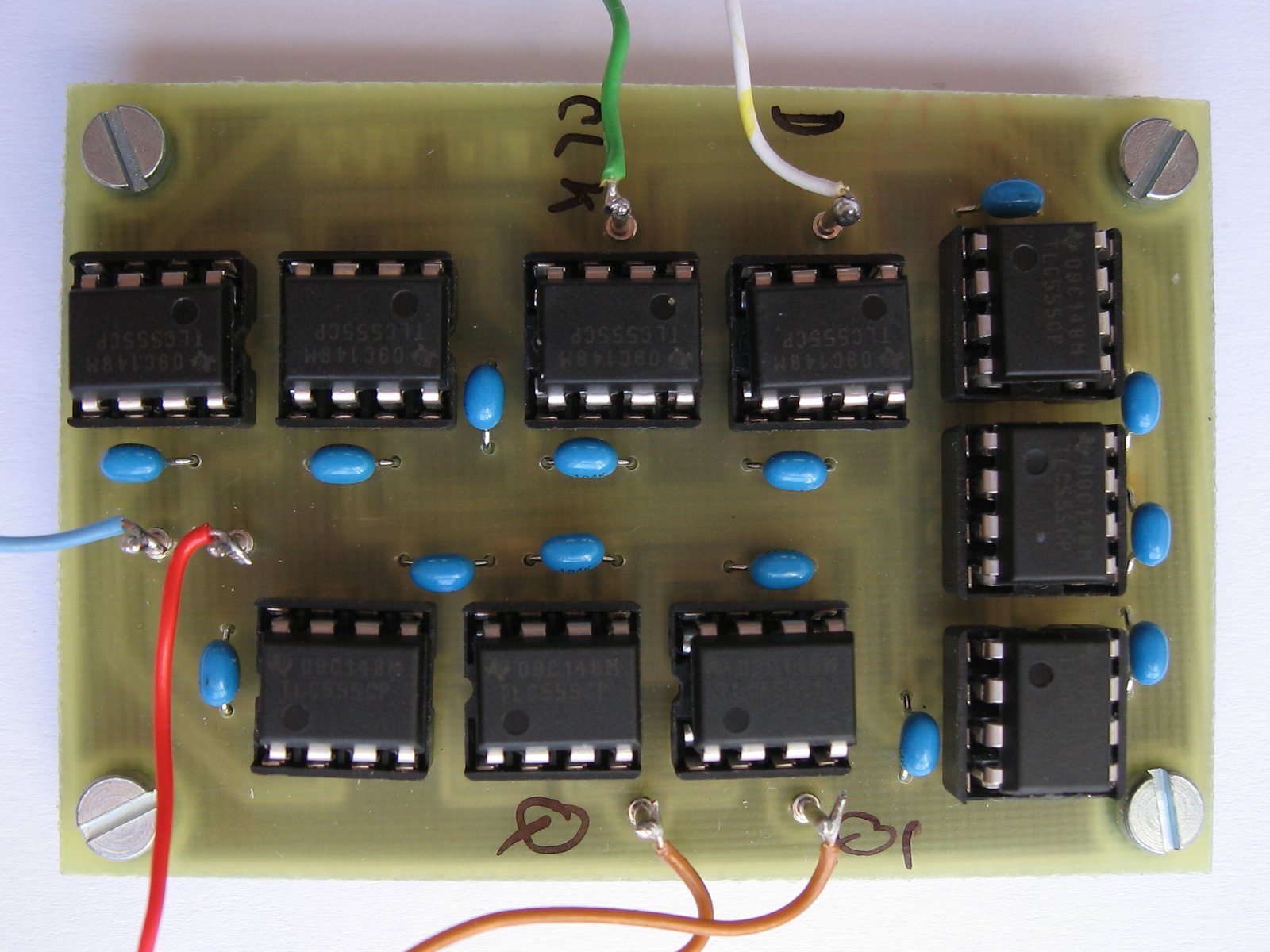
Figure 3.2. Photographs of D flip-flop
test
board (click for larger images)
First,
I tested the board without any decoupling capacitors:
I got best results with TLC555CP again, the
flip-flop worked at 100%.
The outupt state occassionally glitched with LMC555CN.
When I used NE555P, it turned into random state generator
again.
It didn't work at all with LM555N.
So I added the decoupling capacitors to see what
will happen... and it did not
help! I got exactly the same behavior as above.
In this video, I demonstrate how the D flip-flop works in static mode
with TLC555CP:
Unfortunately, when I connected the D and Q
signals together to make a frequency divider, the circuit
again spontaneously
oscillated when the CLK input was held low. That was
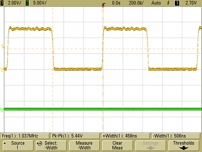
exactly the same behavior I encountered on the breadboard. Oscilloscope
screenshot with these oscillations is in figure 3.3 and their
frequency is about 1 MHz. Unfortuantely, adding all 14 decoupling
capacitors to the board did nothing to improve things. Therefore, I
must sadly report that the circuit in figure 2.5 works like D
flip-flop, but cannot be employed as a frequency divider. To say the
truth, I'm not sure why the circuit oscillates. My best guess is that
it is caused by many non-symetric propagation delays which are
introduced by the 555 inverters. In other words, whereas the flip-flop
in figure 2.1b is symmetrical and so are all propagation delays within
it, my 555 flip-flop is not. I guess this could be corrected by adding
non-inverting (buffer) 555s to some interconnects, but I really don't
feel like doing this. If you succeed in this, let me know.
Figure 3.3. Spontaneous
oscillation of frequency divider as seen on Q output
4 Test of modified 555 inverters
As
I described in chapter 3, the 555 inverters were quite sensitive to the
part number of the actual 555 used - they worked with some and failed
with others. I came to think that the inverter in figure
2.3 may
not be the best implementation, because this
site
recommends a slightly different circuit. The difference is that pin 6
is not connected permanently to VCC, but together with pin 2 represents
the inverter's input. The modified circuit is in figure 4.1. This
circuit behaves more like Schmitt inverter - its input has a
voltage hysteresis between 1/3 and 2/3 VCC.
Figure 4.1. Modified schematic
of 555 inverter
I
made this inverter modification to the test board - I simply cut pins 6
from the VCC plane and connected them with pins 2 by short pieces of
wire. Photograph of the modified board is in figure 4.2.
Unfortunately, this modification did not help much:
It still didn't work at all with LM555N. The inverters
worked this time, but the D flip-flop was permanently stuck in one
state. I found out that when I replaced IC6 with other 555 type, the
circuit worked. So I can safely say that LM555N definitely behaves
differently than other 555 ICs.
It still behaved more like random state generator with
NE555P.
It began to work reliably with LMC555CN.
It worked reliably with TLC555CP as before.
But most importantly, the
flip-flop still oscillated when connected as a frequency divider.
So practically the only improvement was that the flip-flop now worked
100% reliably with LMC555CN.
5 Conclusion
The
purpose of this small project was to create a true edge-trigerred D
flip-flop from 555 ICs. The flip-flop really works, but only in static
mode. It cannot be used as a frequency divider, because it
spontaneously oscillates in this
mode. And since I created the flip-flop exactly because I wanted a
frequency
divider, I must call this project a failure. However, creating the D
flip-flop was still an interesting exercise and I think
someone
might like it anyway.
I
also found out that my flip-flop works only with certain 555 types. In
the end, I was able to make it work with both CMOS types I had, but
only after I modified the inverters according to schematic in figure
4.1. And conversely, the flip-flop failed to work with both bipolar 555
types, no matter what I tried. Interestingly, when I added the
decoupling capacitors to the test board, nothing had changed.